What is graphene?
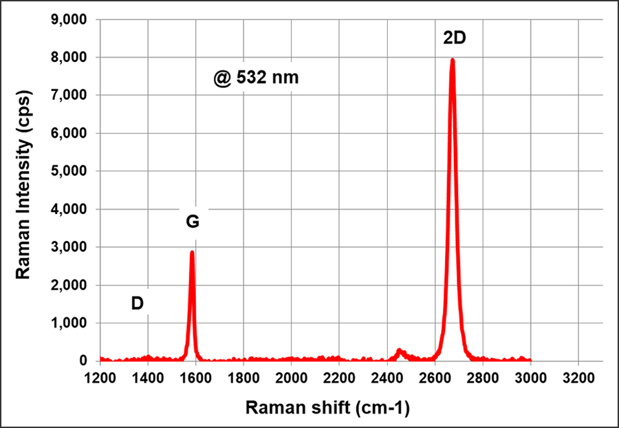
 Graphene is a 2D material which exhibits extraordinary mechanical, electrical, thermal, and optical properties. It is a sheet of closely packed carbon atoms that form a hexagonal crystal lattice. The controlled growth is performed by chemical vapor deposition processes.
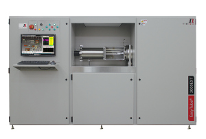
What can our FirstNano® systems do?
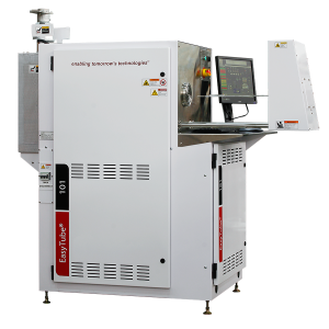
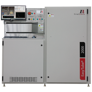
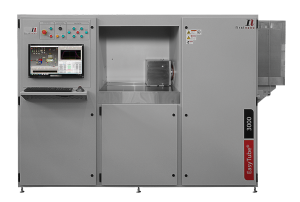
The FirstNano® EasyTube® range of turn-key CVD systems are designed for graphene growth for R&D and pilot production. Based on our advanced EasyTube® CVD platform, the systems are enhanced for high quality growth.
Click on images to enlarge.
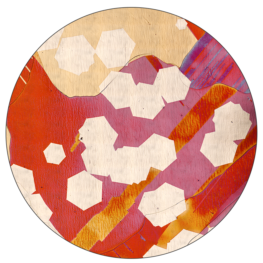
PATENT PENDING EasyGraphene™ Enclosure Box
Our patent pending hardware and process solutions enable a wide process window for mm-sized single crystal graphene grains on copper. System maintenance is reduced by minimizing substrate (e.g. copper) coating on the inside of the process tube.
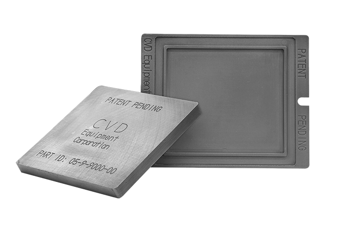
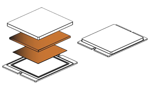
The EasyGraphene™ enclosure box sample holder design acts as a thermal integrating sphere, achieving excellent thermal uniformity. Annealing with the enclosure box produces large single crystal copper grains on the order of the total size of the sample.
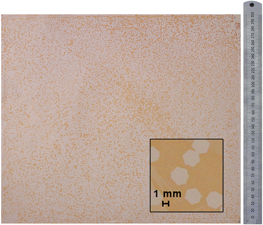
Diffusion of the process gasses into the enclosure box keeps impurities out and provides a uniform precursor concentration (no depletion seen even at sample sizes >= 300 mm x 300 mm). We have demonstrated uniform growth of mm-sized single crystal hexagonal graphene domains accross a 300 mm x 300 mm growth area.
How is graphene applied commercially?
Graphene is manufactured world-wide. It is a new material with many promising applications in a range of industries, including composites, functional coatings, batteries, high-speed electronics, gas sensors etc. It is a transparent conductor which could replace costly indium tin oxide (ITO). Graphene is also flexible, opening up the possibility for flexible touch screen electronics. Graphene is also impermeable to gasses and liquids, making it a candidate for applications in water filtration, treatment, and desalination.
FirstNano® system platforms configurable for graphene growth.
EasyTube® 101 (25 mm x 50 mm Substrate)
EasyTube® 2000 (50 mm x 50 mm Substrate)
EasyTube® 3000 (100 mm x 100 mm Substrate)
EasyTube® 3000EXT (150 mm x 150 mm Substrate)