What are semiconducting nanowires?
![]() One-dimensional semiconducting nanowires allow for device engineering of next generation micro-electro-mechanical systems (MEMS) and optoelectronic devices. Our FirstNano® EasyTube® process equipment is used worldwide for advanced research and development of semiconducting nanowires and nanotubes. Example materials include silicon nanowires (SiNWs), silicon germanium nanowires (SiGe NWs), zinc oxide nanowires (ZnO NWs), and gallium nitride nanowires (GaN NWs).
One-dimensional semiconducting nanowires allow for device engineering of next generation micro-electro-mechanical systems (MEMS) and optoelectronic devices. Our FirstNano® EasyTube® process equipment is used worldwide for advanced research and development of semiconducting nanowires and nanotubes. Example materials include silicon nanowires (SiNWs), silicon germanium nanowires (SiGe NWs), zinc oxide nanowires (ZnO NWs), and gallium nitride nanowires (GaN NWs).
What can our FirstNano® systems do?
FirstNano® EasyTube® systems can be configured for a wide range of processes and chemistry for nanowire production. The nanowire/nanotube growth proceeds via the vapor-liquid-solid (VLS) CVD mechanism, whereby precursors are introduced to the reactor and the desired element alloys with metal catalyst nanoparticles. By adding more and more of the semiconductor element to the alloy, the element precipitates from the alloy and nucleates at the interface with the substrate surface. Subsequent addition of the element to the alloy feeds the growth, resulting in one-dimensional structures with controllable diameters, lengths, and crystallinity.
How are semiconducting nanowires applied commercially?
Semiconducting nanowires can be engineered as microscopic light sources for optical computing. They can also be used in solar photovoltaic devices where the 1D structures can lead to higher efficiency energy conversion. Nanoscopic 1D structures can be integrated in atomic force microscopy (AFM) and Raman spectroscopy to achieve higher analytical resolution. Silicon nanowires have many applications in biotechnology, including cell interfacing, DNA and protein delivery, biosensors, and imaging.
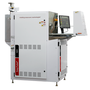
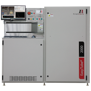
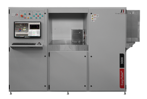
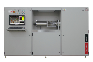
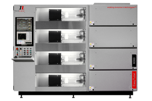
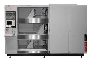
FirstNano® system platforms configurable to grow semiconducting nanowires.

