What are transition metal dichalogenides (TMDs)?
 Two-dimensional atomic layers of transition metal dichalcogenides (TMDs) such as molybdenum disulfide (MoS2) and tungsten diselenide (WSe2) exhibit extraordinary optoelectronic properties. Applications for these materials include high speed electronics, flexible devices, next generation solar cells, and touch screen display panels.
What can our FirstNano® systems do?
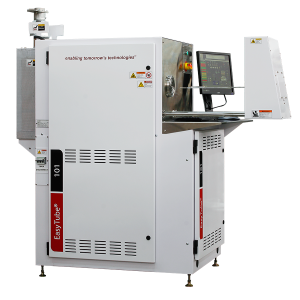
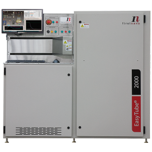
The FirstNano® EasyTube® 101 and 2000 can be configured for solid source and designed to grow 2D layers of TMDs for advanced research applications. The system can perform chemical vapor deposition, chemical vapor transport, and selenization / sulfurization processes. It includes a fully capable safety system. The CVDWinPrC™ instrument control and process editing software suite, included as standard, is equivalent to that used on our industry-ready production equipment.
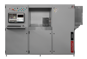
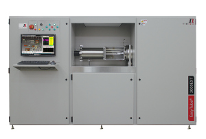
The EasyTube® 3000 and 3000EXT can be configured for and designed for wafer-scale growth of uniform 2D TMD layers with abrupt interfaces for the advanced optoelectronics research and development user. The systems include metal organic vapor and hydride gas delivery. Our EasyTube® MOCVD platform is widely used in universities and industry.
How are TMDs applied commercially?
TMDs are rapidly gaining popularity for researchers worldwide. They are semiconducting materials that, unlike graphene, can be grown directly on insulating substrates. 2D atomic layers of TMDs have a direct bandgap that can be tuned by increasing the numer of atomic layers. There are many potential commercial applications for these devices, including flexible integrated circuits and next generation optoelectonics.
FirstNano® system platforms configurable for depositing layers of TMDs.


